


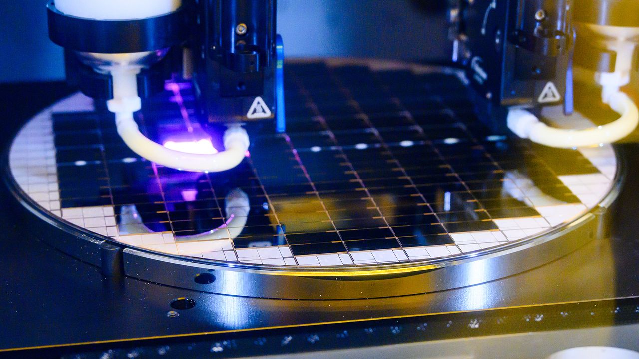
Last week, ASML introduced the Twinscan XT:260 lithography scanner, the industry’s first scanner that has been designed from the ground up for advanced 3D packaging, marking a new era in fab tools.
Advanced packaging technologies like TSMC’s Chip-on-Wafer-on-Substrate (CoWoS) are crucially important to achieve the performance scaling necessary to develop artificial intelligence and to evolve supercomputers.
You may like
“In line with our plans to support our customers in the 3D integration space, we shipped ASML’s first product serving Advanced Packaging, the Twinscan XT:260, an i-line scanner offering up to 4x productivity compared to existing solutions.”, ASML posted in its Q3 2025 financial results.
The Twinscan XT:260
ASML’s Twinscan XT:260 is an i-line (365 nm) step-and-scan lithography system that processes 300-mm wafers and weds the precision of previous-generation front-end lithography tools with the productivity and flexibility of back-end tools. TSMC claims this provides four times higher productivity compared to ‘competing steppers’ used for advanced packaging technologies, such as Canon’s FPA-5520iV. ASML never named the exact competing product, but Canon’s FPA-5520iV is a good bet.
(Image credit: ASML)
The key advantage of the tool compared to some of the existing machines used for advanced packaging is that it supports a high-dose exposures (340 mJ is mentioned, though it is usually tunable) and a 52 mm × 66 mm image field, enabling the tool to process up to 3,432 mm^2 interposers (4X EUV reticle size) without field stitching, which reduces complexity and speeds up the production cycle. For the sake of truth, it should be noted that Canon’s FPA-5520iV LF2 Option supports a 52 mm × 68 mm image field, but this is a stepper, not a scanner.
The system delivers 400 nm resolution, a 35 nm overlay, and offers a large depth of focus (11 µm at 1 µm CD) to enable accurate patterning for redistribution layers (RDLs) through-silicon vias (TSVs), and hybrid bonding structures used by modern packaging methods to integrate multi-chiplet designs. The unit also boasts 775 µm through-silicon alignment capabilities to make it particularly suited for bonded or non-planar wafers, which are common in 3D stacking.
The Twinscan XT:260 relies on ASML’s dual-stage platform, so it can expose one wafer while simultaneously aligning the next, which significantly increases its performance. Speaking of performance, the machine can process up to 270 wafers per hour (at a 340 mJ dose) and handle thick (0.775 mm – 1.7 mm) or warped (1 mm) wafers.
With a 400 nm resolution, 35 nm overlay, and the ability to handle thick or warped wafers (up to 1.7 mm), the XT:260 is optimized for technologies Intel’s Foveros, TSMC’s CoWoS and System-on-Integrated-Chips (SoIC), as well as other high-density die-stacking or interposer technologies which require precise alignment through silicon.
The Twinscan XT:260 is positioned below the Twinscan XT:400M, the company’s most basic i-line scanner used for chipmaking on mature nodes, but which may be an overkill for chip packaging on advanced nodes for now. Keep in mind that there are plenty of ASML’s PAS 5500 i-line steppers that are used for ‘more-than-Moore’ applications, which is the company’s convoluted way of pointing towards advanced packaging.
You may like
Compared with Canon’s FPA-5520iV and the long-standing PAS 5500 i-line steppers, which have been widely used for CoWoS and fan-out packaging, the XT:260 represents a major leap in both productivity and precision. While the aforementioned tools rely on step-and-repeat exposure with limited throughput and field size (PAS 5500 only), the XT:260 introduces a scanner architecture with continuous wafer movement, advanced alignment optics, and automation suitable for high-volume 3D integration, which will be particularly important given that demand for advanced packaging is increasing.
The big picture
ASML’s Twinscan XT:260 is the industry’s first lithography scanner designed specifically for advanced packaging. It’s not the only lithography scanner aimed at advanced packaging, though. The semiconductor industry has a choice: Use new tools like the Twinscan XT:260, or repurpose existing tools designed for front-end chip manufacturing for advanced packaging. If ASML’s estimations are correct, using this specific tool will be technically beneficial, but may come at significant expense.
(Image credit: TSMC)
Previous-generation front-end lithography, etch, and deposition tools offer sub-micron precision, but need ultra-clean processing environments that ensure tight overlay and defect control. This is because they produce thousands of interconnects linking chiplets and HBM stacks in 2.5D, and eventually 3D System-in-Packages (SiPs).
However, these front-end tools are far more expensive — both in terms of price, performance, and total cost of ownership — than what is typically required for back-end packaging steps. Hence, using them in packaging lines drives up cost and limits output. One advantage of using them is that developers, process control engineers, and technicians at Intel and TSMC are familiar with those tools, which almost certainly guarantees good yields and fast ramp-ups. However, it comes at a high cost and a relatively long production cycle.
With tools like ASML’s Twinscan XT:260, wafer-level stages that demand extreme precision — TSV formation, RDL patterning, and hybrid bonding — will get faster and therefore cheaper. This will set the stage for the broader adoption of advanced packaging technologies in several years. It’ll likely take some time for chipmakers like Intel, Samsung, and TSMC, or OSAT companies like ASE, Amkor, and JCET, to integrate the lithography system into their process technologies and flows.
There are a lot more tools to be designed specifically for advanced packaging. Advanced packaging techniques still rely on ‘classic’ back-end tools for underfill, molding, ball attach, and many other operations. This hybrid flow balances cost with accuracy: front-end-grade tools where micron (or even nanometer) alignment matters.
As advanced packaging facilities use front-end tools (with appropriate costs), the boundary between foundries and OSATs is blurring. TSMC’s CoWoS and SoIC facilities are filled with wafer fab equipment from ASML, Applied Materials, Canon, KLA, Lam Research, and Tokyo Electron, and usually cost north of $3 billion, the cost of a chip fab in the early 2010s. This is going to continue as more WFE makers set to produce tools specifically tailored for advanced packaging in the coming years and quarters.
Follow Tom’s Hardware on Google News, or add us as a preferred source, to get our latest news, analysis, & reviews in your feeds.
