

Chinese semiconductor start-up Prinano announced that it has successfully validated the mass production of photonic chips without using the industry-standard lithography equipment. According to an SCMP report, the company said in a WeChat post on Friday, June 5th, that it had made 8-inch optical chip wafers in collaboration with Shenzhen Litra Technology. The company said it achieved this while “completely avoiding” the need for deep-ultraviolet lithography (DUV), a significant breakthrough in China’s push to reduce its dependence on ASML lithography tools, which remain subject to export restrictions.
Go deeper with TH Premium: Chipmaking
(Image credit: tsmc)
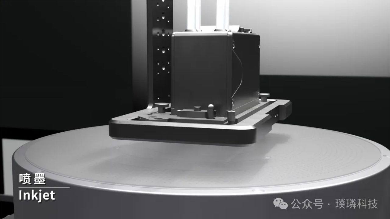
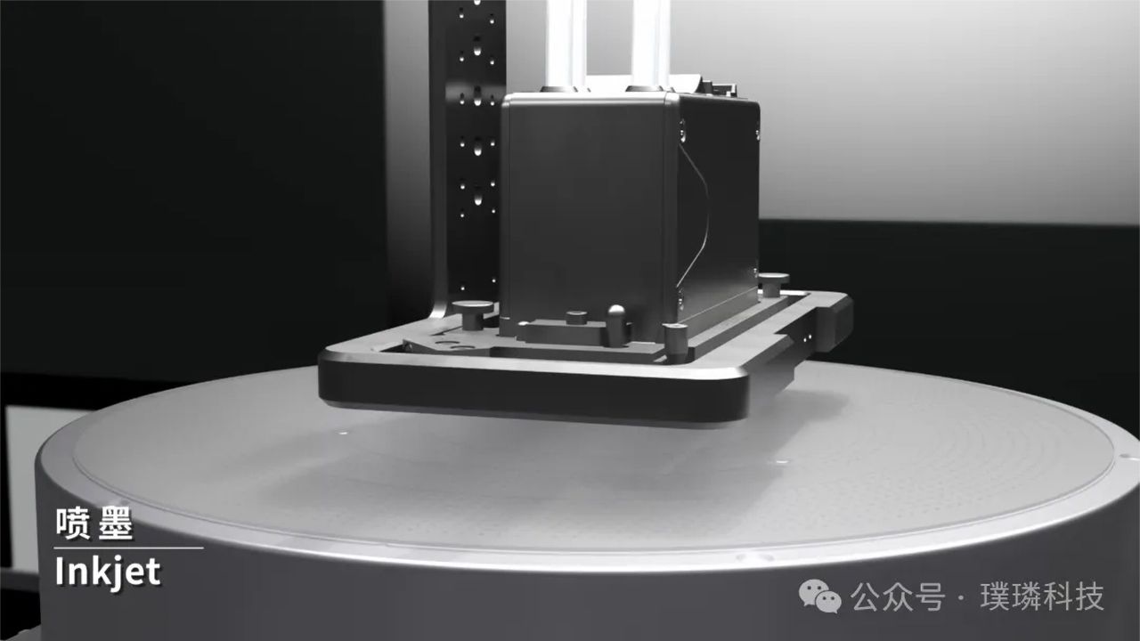
Instead of conventional optical lithography, Prinano said it used its PL-AS vacuum air-cushion nanoimprint lithography (NIL) system, which, according to the company, can reduce manufacturing costs to roughly one-tenth that of traditional DUV-based processes, while supporting wafer-level production of photonic chips.
Modern chips are typically produced using highly sophisticated DUV or more advanced EUV (extreme ultraviolet) systems that project circuit patterns onto silicon wafers using light. These machines contain some of the most complex optics ever built and can cost hundreds of millions of dollars. Nanoimprint lithography takes a very different approach. Rather than projecting patterns using light, it physically presses nanoscale structures into a specially prepared resist layer, basically stamping microscopic patterns directly onto the wafer surface. This process eliminates the need for many of the expensive optical systems required by conventional lithography equipment.
Latest Videos From
Nanoimprint lithography has long been viewed as a potential alternative to conventional optical lithography because of its potential for lower costs and extremely high pattern resolution. However, despite its promise, the technology has struggled to achieve widespread adoption in semiconductor manufacturing due to concerns about defect rates, template wear, throughput, and production yields, all of which become increasingly important in high-volume manufacturing environments.
Founded in 2017, Prinano has spent the past several years working to overcome those limitations by developing its own nanoimprint lithography ecosystem. The company took a significant step in 2025 when it announced the delivery of what it described as China’s first semiconductor nanoimprint lithography system to a domestic customer, marking an early effort to commercialize the technology.
You may like
The company’s latest announcement suggests it may have progressed beyond equipment development and pilot deployments. According to Prinano, its PL-AS vacuum air-cushion nanoimprint lithography platform incorporates wafer-level pressure control, customized double-layer imprinting materials, and proprietary process technologies capable of producing sub-10-nanometer features. The company now claims those developments have enabled the successful validation of wafer-scale photonic chip production on 8-inch wafers.
Importantly, Prinano is not attempting to replace the production of cutting-edge processors or AI accelerators. Instead, the company’s announcement focuses on photonic chips, a category of semiconductors that manipulate light rather than electrical signals. These devices are widely used in fiber-optic communications, data center interconnects, sensing systems, and LiDAR technologies.
Photonic chips are considered particularly well suited to nanoimprint lithography because many of their critical structures, including waveguides, gratings, and ring resonators, consist of repeating nanoscale patterns that can be replicated efficiently through imprinting techniques. This characteristic makes them a more practical near-term application for NIL than advanced logic chips, where defect rates and alignment requirements are far more demanding.
Another noteworthy detail is the use of 8-inch wafers. While leading-edge processors are increasingly manufactured on larger 12-inch wafers, 8-inch wafers remain widely used across specialized sectors such as compound semiconductors and power electronics. Demonstrating production on full 8-inch wafers suggests the process has moved beyond laboratory-scale demonstrations and into a format more compatible with commercial manufacturing.
The development also highlights China’s broader search for alternative semiconductor manufacturing pathways amid ongoing export restrictions. Access to advanced lithography equipment from ASML — required for EUV and DUV — has been increasingly constrained under US-led controls, prompting Chinese companies to explore alternative approaches ranging from advanced packaging technologies to new chip architectures and novel manufacturing methods. Huawei recently announced a new LogicFolding chip architecture that allows the company to develop high-performance processors without relying on restricted EUV lithography machines.
Significant questions remain about Prinano’s announcement. While the claims have been validated in mass production, the company did not disclose production volumes, yield rates, defect densities, customer shipment data, or independent third-party validation. These metrics are critical for determining whether a semiconductor manufacturing technology is commercially viable rather than merely technically feasible.
Follow Tom’s Hardware on Google News, or add us as a preferred source, to get our latest news, analysis, & reviews in your feeds.
